

Please ensure Javascript is enabled for purposes of website accessibility

What Are the Top Solar Cell Carrier Types?

Solar manufacturing runs at a scale where small handling choices matter. The IEA PVPS report Trends in Photovoltaic Applications 2024 estimates that global installed solar capacity reached about 1.6 terawatts in 2023, with roughly 446 gigawatts added that year. Those figures describe the market, not carrier performance. But they help explain why reliable wafer handling is a practical concern across production lines.

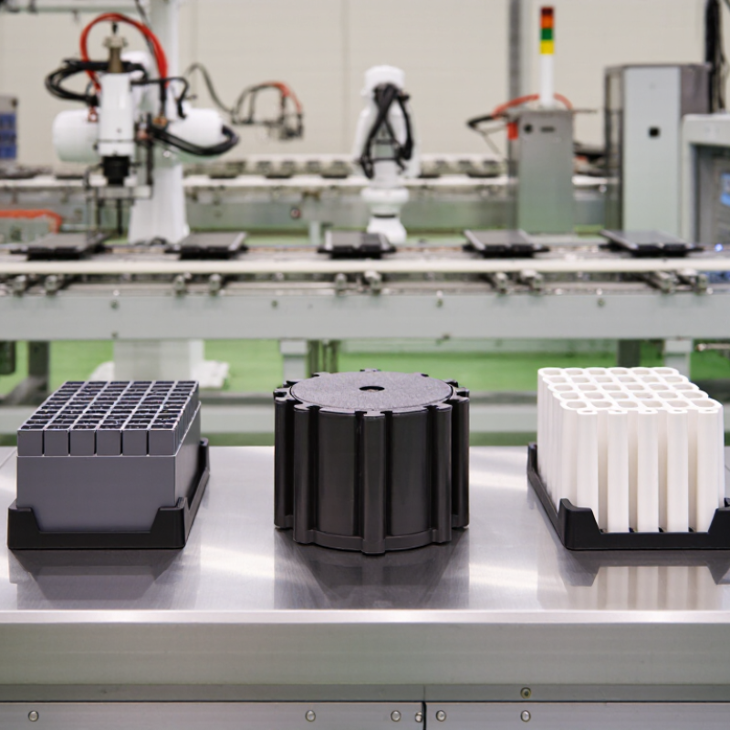
Here, a Solar Cell Carrier means a fixture or vessel that supports wafers during manufacturing. Common options include quartz boats, silicon carbide carriers, graphite fixtures, ceramic carriers, and polymer cassettes. Their suitability depends on the process: high-temperature steps, chemical exposure, contamination limits, and wafer dimensions all influence the choice. A quartz boat may suit one stage, while a polymer cassette may be used for cooler handling. Details matter.

Industry roadmaps such as the International Technology Roadmap for Photovoltaic (ITRPV) track ongoing changes in wafer formats and production technology. Those changes can affect carrier compatibility, so a material ranking alone is not enough. A tidy list can mislead. Buyers and engineers should check operating conditions, cleanliness requirements, maintenance needs, and supplier specifications before comparing options. The carrier that looks simplest may still become a bottleneck. This guide compares the main types and the trade-offs behind them, while recognizing that no single carrier fits every factory or process.
What Are the Top Solar Cell Carrier Types?

How Solar Cells Generate Charge Carriers

When sunlight reaches a solar cell, photons transfer energy to the semiconductor. In silicon, photons need at least about 1.12 electron volts to cross the band gap. Absorption can lift an electron into a mobile energy state, leaving behind a positively charged “hole.” These are the cell’s charge carriers. If a photon’s energy is too low, it may pass through without creating a pair. Excess energy usually becomes heat. Not every absorbed photon produces useful current.

A p-n junction creates an internal electric field that pushes electrons and holes in opposite directions. Metal contacts collect them, and their movement through an external circuit supplies electrical current. NREL’s Best Research-Cell Efficiency Chart reports a laboratory crystalline-silicon cell efficiency of about 27.3%. That is a research result, not a rooftop guarantee. Defects, heat, shading, and resistance can all reduce carrier collection. IEA PVPS’s Trends 2024 report estimates that global cumulative solar capacity exceeded 1.6 terawatts in 2023, making small efficiency losses meaningful at scale. Still, efficiency figures alone do not show how well a cell handles changing light or temperature. That deserves attention.

Electrons as Negative Charge Carriers

In a solar cell, electrons are the main negative charge carriers. They already exist inside the semiconductor, often silicon. When sunlight delivers enough energy, an electron can break free from a bond. This creates two mobile carriers: a negative electron and a positively charged hole. The hole is not a tiny particle; it describes an electron’s missing place. Both carriers matter.

An internal electric field helps separate electrons from holes. The electrons travel toward one contact, then move through an external circuit, powering a device before returning to the cell. Conventional current is described in the opposite direction. Small detail, big difference. The simple diagram is useful, but incomplete: heat, material defects, and recombination can prevent some electrons from reaching the contact. A bright patch of sunlight therefore does not mean every freed electron becomes useful current. Carrier movement depends on the cell’s structure and condition, too. That distinction is easy to overlook.

Solar Cell Charge Carriers: Electrons and Holes

In a solar cell, electrons carry a charge of −1 elementary charge. A hole—the absence of an electron in a material—acts as a positive carrier with a charge of +1 elementary charge.

Holes as Effective Positive Charge Carriers

What Are the Top Solar Cell Carrier Types?

Holes as Effective Positive Charge Carriers

When sunlight enters a solar cell, its photons can transfer energy to electrons. An energized electron may leave its position in a material’s valence band and move into a higher-energy state. The empty position left behind is called a hole. It behaves like a positive charge carrier, even though it is not a separate, positively charged particle. That is the key. As nearby electrons shift to fill the vacancy, the hole appears to move through the material. This movement helps carry electrical current toward the cell’s contacts.

A hole’s usefulness depends on how easily it moves and how long it survives before recombining with an electron. Material quality, defects, and interfaces can all affect that journey. In practice, a cell can generate plenty of carriers yet perform less well if holes become trapped or recombine too quickly. The details vary by cell design, so “good hole transport” is not one universal number.

Tips: When assessing a solar-cell material, look at hole mobility and recombination together. Check whether the measurement reflects real device conditions. A tidy lab result may not tell the whole story. It is worth questioning that.

Majority and Minority Carriers in Semiconductor Layers

In a doped semiconductor layer, majority carriers are the more abundant charge carriers. In n-type silicon, electrons are the majority carriers; in p-type silicon, holes are. The opposite carrier is called the minority carrier. The labels are relative. Light absorbed by a solar cell creates electron–hole pairs, and the junction’s electric field helps separate them before they recombine.

Minority-carrier behavior matters because those carriers must travel toward a contact to contribute to current. Defects, impurities, or poorly passivated surfaces can shorten their lifetime, reducing collection.

NREL’s Best Research-Cell Efficiency Chart reports a 27.3% research-cell efficiency for crystalline silicon; that result reflects many design factors, not carrier concentration alone.

In practice, engineers use measurements such as carrier lifetime and recombination rates to assess how effectively a layer preserves useful carriers. A clean textbook picture can be misleading: real cells contain interfaces, and carriers may behave differently near them. A thin, well-passivated layer can help. But the best approach depends on the material stack and the path carriers must travel.

Excitons and Carrier Separation in Advanced Solar Cells

An exciton is a bound electron–hole pair created when a semiconductor absorbs light. It is not a separate charge carrier. Useful current begins when the pair separates, leaving mobile electrons and holes. In silicon, these pairs usually separate readily. In many organic absorbers, stronger binding makes interfaces crucial. A donor–acceptor boundary can help pull the electron away. Too much energy offset, though, can waste voltage.

Halide perovskites often sit between these cases. Their excitons can dissociate at room temperature, but defects and grain boundaries may trap carriers. A device must balance light absorption, carrier travel, and charge extraction. Picture a thin film under sunlight: electrons and holes need a clear route to opposite contacts. A rough interface can instead encourage recombination. Small material changes matter.

NREL’s Best Research-Cell Efficiency Chart records a 34.6% perovskite–silicon tandem result in 2024, showing the potential of stacked absorbers. IEA PVPS’s Snapshot of Global PV Markets 2024 estimated about 447 GW of new solar capacity worldwide in 2023. That scale makes efficiency valuable, but a record cell does not prove long-term stability or manufacturing yield. I would treat peak performance as evidence of progress, not a guarantee of field results.

What Are the Top Solar Cell Carrier Types? - Excitons and Carrier Separation in Advanced Solar Cells

Carrier or Excited State Electrical Charge Typical Solar-Cell Context Role in Photovoltaic Operation Separation and Collection Useful Energy-Scale Reference
Electron Negative (−e) Crystalline silicon, III–V semiconductors, perovskites, and organic photovoltaics A mobile charge carrier in the conduction band or an electron-transporting state. An electric field, selective contact, or material interface directs electrons toward the electron-collecting contact. Its transport and collection depend on band structure, mobility, defects, and device architecture—not on a single universal energy value.
Hole Positive (+e) The same broad range of semiconductor solar cells as electrons The mobile absence of an electron in an otherwise occupied valence-band or molecular state. Fields and hole-selective contacts guide holes toward the opposite contact from electrons. Hole transport is material- and defect-dependent; the hole is a quasiparticle, not a positively charged proton.
Exciton Neutral bound electron–hole pair Commonly important in organic semiconductors; also occurs in inorganic semiconductors and perovskites Light absorption can create an electron and hole that remain Coulomb-bound as an excited state. In many organic cells, excitons diffuse to a donor–acceptor interface, where charge transfer can separate the pair. In other materials, thermal energy or internal fields may enable dissociation. Approximate binding-energy examples: about 0.3–1 eV in many organic semiconductors; about 14.7 meV in silicon and about 4.2 meV in GaAs. Values vary with material and conditions.
Charge-transfer (CT) state A spatially separated electron and hole; the pair may still be Coulomb-bound Most often discussed at donor–acceptor interfaces in organic solar cells An intermediate state formed when an electron transfers to an acceptor while the hole remains on the donor. The CT state may separate into mobile charges or recombine; energy-level offsets, interfacial structure, and local disorder influence the outcome. Its energy and degree of binding are system-specific; there is no single representative value for all interfaces.
Polaron Usually charged: an electron polaron or a hole polaron Organic semiconductors and some soft-lattice materials, including metal-halide perovskites A charge carrier coupled to a local or extended distortion of the surrounding material. Polaron formation can affect carrier mobility, screening, trapping, and recombination; its effect depends on the material and timescale. Polaron size and stabilization energy vary substantially; a polaron is not a separate fundamental charge from an electron or hole.

Note: Electrons and holes are charge carriers; excitons and charge-transfer states describe excited electron–hole configurations. Whether light-generated pairs need an interface to separate depends on the material and device design.